Judy Lau
Staff Writer
Illustration by Silvia Quach, Staff Illustrator
New research at Rice University shows how water can be used in creating long graphene nanoribbons less than 10 nanometers wide.
The discovery by lead author Vera Abramova and co-author Alexander Slesarev, both graduate students in the lab of Rice chemist James Tour, appears this month in the American Chemical Society journal. The technique builds on the discovery that the meniscus, the curved surface of water at its edge, can be an effective mask on which to make nanowires.
The Rice team uses a technique called meniscus-mask lithography. This process involves adding and then removing materials in a sequence that leaves the meniscus covering the wire and climbing the side of the metal mask that, when etched away, leaves the nanowire standing alone.
“They can never take advantage of the smallest nanoscale devices if they can’t address them with a nanoscale wire,” said Tour. “Right now, manufacturers can make small features, or make big features and put them where they want them. But to have both has been difficult. To be able to pattern a line this thin right where you want it is a big deal because it permits you to take advantage of the smallness in size of nanoscale devices.”
Current approaches to making such small wires take several paths. Lithography, the standard method for etching integrated circuits, is approaching the physical limits of its ability to shrink them further. Bulk synthesis of semiconducting and metallic wires is possible but difficult.
The meniscus-mask process is promising because it makes circuits even smaller. Integrated circuit fabrication allows for signal wires that approach 10 nanometers, visible only with powerful microscopes. These paths connect billions of transistors in modern electronic devices.
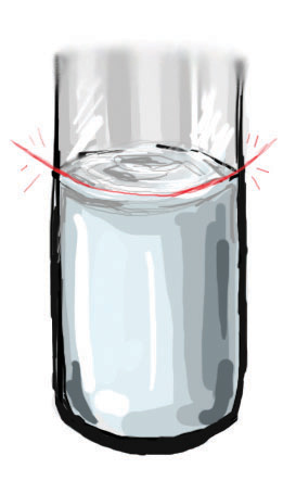
Although water’s tendency to adhere to surfaces is often annoying, it is essential to the process in creating these nanowires by making patterns. The water molecules gather wherever a pattern joins the target material and forms a curved meniscus created by the surface tension of water.
“There are big machines that are used in electronics research that are often heated to hundreds of degrees under ultrahigh vacuum to drive off all the water that adheres to the inside surfaces,” said Tour. “Otherwise there’s always going to be a layer of water. In our experiments, water accumulates at the edge of the structure and protects the graphene from the reactive ion etching. So in our case, the residual water is the key to success.”
Abramova and Slesarev fabricated nanoribbons by inverting a method developed by another Rice lab to make narrow gaps in materials. The original method used metals to form an oxide layer that expands and shields material just on the edge of the metal mas.
It took two years to develop and test the meniscus theory, during which the researchers confirmed potential to create 10-nanometer wires from other materials, such as platinum. The researchers are working to better control the nanoribbons’ width, and they hope to refine the edges of the wire to help dictate their electronic properties.
“This could have huge ramifications for chip production since the wires are easily made to sub-10-nanometer sizes,” said Tour. “There’s no other way in the world to do this en masse on a surface.”
Tour said the process should work with modern fabrication technology with no modifications to existing equipment and minimal changes in fabrication protocols. No new tools are needed.
“With this study, we figured out you don’t need expensive tools to get these narrow features,” said Tour. “You can use the standard tools a microfabrication line already has to make features that are smaller than 10 nanometers.”
The Air Force Office of Scientific Research and the Office of Naval Research Multidisciplinary University Research Initiative Graphene Program supported the research.


“no modifications to existing equipment and minimal changes in fabrication protocols. No new tools are needed.” so I take it that means that any reactive ion etching system will be able to create wire with water that is just 10 nm wide?
Comments are closed.